Monday, March 30, 2015

Introduction to SDR: Part2


Changing Radio Configuration parameters

We can change and apply radio hardware parameters and tune radio properties before transmitting or receiving signals.Following properties can be changed:
  • Baseband Sampling Rate and Filter Chains
  • DC Blocking
  • Intermediate Frequency Tuning
Now let us discuss all of them in more detail.

1. Baseband Sampling Rate and Filter Chains: 

          To set up the baseband sampling rate and filter chains for radio hardware, use a combination of            two parameters or properties.
  • For a receiver System object™ or block, set both the ADC rate and decimation factor.
  • For a transmitter System object or block, set both the DAC rate and interpolation factor.

Decimation Factors: 

The FPGA image includes a decimation filter chain, which is controlled by the Decimation Factor parameter or property on the transmitter block or System object. 
The filter chain consists of a CIC filter followed by two halfband filters.


The first halfband filter has a wider transition band and fewer filter weights than the second one.
For this reason, the first halfband is called halfband lightweight (HBL) and the second is called halfband heavyweight (HBH).

The filter chain supports decimation factors from this set of values:

[1:128,130:2:256,260:4:512]

that is,

Any integer from 1 to 128
A multiple of 2 from 130 to 256
A multiple of 4 from 260 to 512

The CIC filter has a variable decimation factor (CIC rate) from 2 through 128, which you can bypass.

Each halfband filter decimates by a factor of 2. You can bypass these filters too. The filters are enabled or bypassed according to these rules:


  • If the decimation factor is divisible by 4, then both HBL and HBH are enabled.
  • If the decimation factor is divisible by 2 and not by 4, then HBL is bypassed and HBH is enabled.
  • If the decimation factor is not divisible by 2, then HBL and HBH are both bypassed.
  • The remaining decimation factor is made up by the CIC filter. If the remaining factor is 1, then the CIC is bypassed.

NOTE: The receiver block or System object incorporates the logic to determine these settings automatically from the specified Decimation factor parameter or property.

Interpolation Factors

The FPGA image includes an interpolating filter chain, which is controlled by the Interpolation Factor parameter or property on the transmitter block or System object.
The filter chain consists of two halfband filters followed by one CIC filter.

The first halfband filter has a sharper transition band and more filter weights than the second one. For this reason, the first halfband is called halfband heavyweight (HBH) and the second is called halfband lightweight (HBL).

The filter chain supports interpolation factors from this set of values:

[1:128, 130:2:256, 260:4:512]

that is,

  • Any integer from 1 to 128
  • A multiple of 2 from 130 to 256
  • A multiple of 4 from 260 to 512


Each halfband filter interpolates by a factor of 2, which you can bypass. The CIC filter has a variable interpolation factor (CIC rate) of from 2 through 128. This filter can also be bypassed. The filters are enabled or bypassed according to these rules:


  • If the interpolation factor is divisible by 4, then both HBH and HBL are enabled.
  • If the interpolation factor is divisible by 2 and not by 4, then HBH is enabled and HBL is bypassed.
  • If the interpolation factor is not divisible by 2, then HBH and HBL are both bypassed.
  • The remaining interpolation factor is made up by the CIC filter. If the remaining factor is 1, then the CIC is bypassed.

Note: The receiver block or System object incorporates the logic to determine these settings automatically from the interpolation factor parameter or property you specify.


2. DC Blocking

Direct conversion receivers often impose a DC bias on the in-phase and quadrature components of the signal. DC bias, if not dealt with, leads to degraded BER performance for QAM systems, and to a lesser extent, PSK systems.

With DC blocking enabled, DC bias is reduced in the I/Q channels of a received complex signal.

The reduced DC bias better enables robust receiver processing

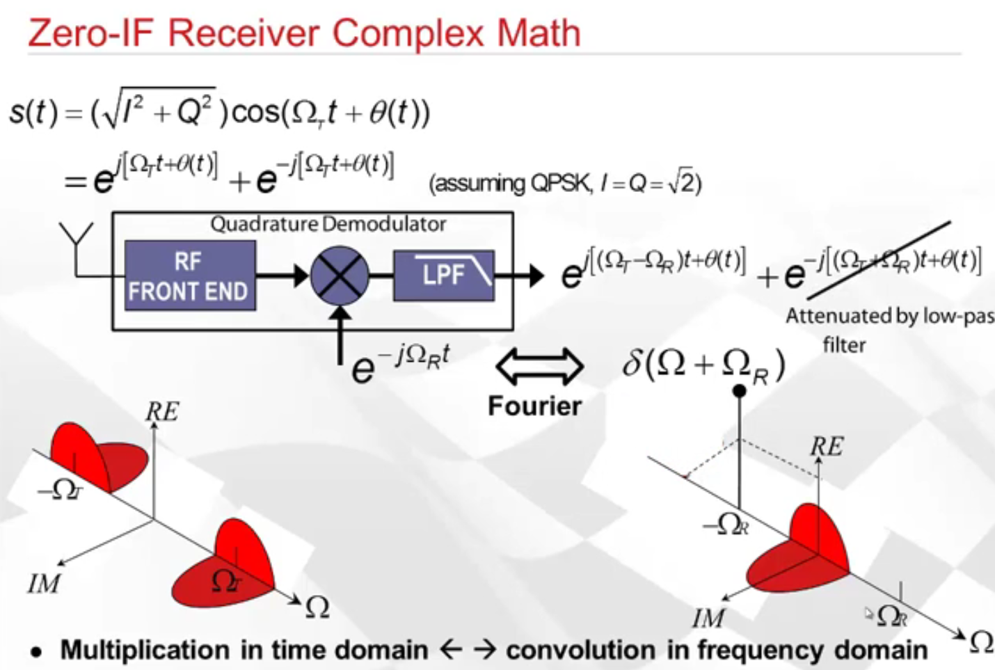
3. Intermediate Frequency Tuning


  • Intermediate frequency (IF) tuning supports second-stage tuning for the transmit and receive data paths. 
  • The tuner is configurable at run time (tunable) and provides finer resolution when compared to the primary tuner on an RF card. 
  • The tuner also enables you to remove unwanted interference from the passband of interest.


--------------------------------------------------------------------------------------------------------------------------

ZedBoard and FMCOMMS1 RevB/C Transmitter


The ZedBoard and FMCOMMS1 RevB/C Transmitter block is a signal source that sends data to a Xilinx® ZedBoard™ with Analog Devices™ FMCOMMS1 RevB/C RF card on the same Ethernet subnetwork.

DATA FLOW FROM MATLAB TO HARDWARE 


Input to Transmitter Block

The input port supports the following complex and real data types:

  • Double-precision floating point
  • Single-precision floating point
  • 16-bit signed integers

NOTE: All input must be framed based.

Output of Transmitter Block

When you select a double or single data type, the complex values are in the range of [-1,1] and converted to int16.
When you select int16, the complex values are 16-bit I and Q samples that are then sent to the radio hardware.

Following are the parameters that need to be set for the transmitter block.


Center frequency (Hz)

The value can be chosen using a Dialog, and specify the center frequency as a double-precision, nonnegative, finite scalar.
The default is 2.4 GHz.
The valid range of values for this parameter is 400MHz–4GHz.

Intermediate frequency (Hz)

The intermediate frequency (IF) tuner allows you to account for the error in tuning between target center frequency and actual center frequency and avoid unwanted interference by shifting the error out of the passband of interest.
The default value is 0 Hz. The valid range of values for this parameter is  to , where  is the digital-analog converter (DAC) rate.

DAC sampling rate (Hz)

Specify the sampling rate as a double precision, nonnegative scalar. The default value is 98 MHz. The valid range of this parameter is 25–125 MHz.

Interpolation factor


Specify the interpolation factor as a double precision, nonnegative scalar. The default is 512.

IMP- The baseband rate is DAC sampling rate divided by the Interpolation factor.


--------------------------------------------------------------------------------------------------------------------------

ZedBoard and FMCOMMS1 RevB/C Receiver


The ZedBoard and FMCOMMS1 RevB/C Receiver block is a signal source that receives data from a Xilinx® ZedBoard™ with Analog Devices™ FMCOMMS1 RevB/C RF card on the same Ethernet subnetwork.

The ZedBoard and FMCOMMS1 RevB/C Receiver block outputs a matrix signal where each column is a channel of data of fixed length. 

The data length port, DataLength, indicates when valid data is present. When the data length port contains a zero value, there is no data. 
You can use the data length with an enabled subsystem to qualify the execution of part of the model.


Output Data:

The output port supports the following complex data types only:

  • Double-precision floating point
  • Single-precision floating point
  • 16-bit signed integers
NOTE:  When you select a double or single data type, the complex values are scaled to the range of [-1,1]. When you select int16, the complex values are the raw 16-bit I and Q samples from the board.

Following are the parameters that need to be set for the receiver block.


Intermediate frequency (Hz)

The intermediate frequency (IF) tuner allows you to account for the error in tuning between target center frequency and actual center frequency and avoid unwanted interference by shifting the error out of the passband of interest. If you choose Dialog, specify the center frequency as a double-precision, finite scalar. The default value is 0 Hz. The valid range of values for this parameter is  to , where  is the analog-digital converter (ADC) rate.

Gain (dB)

Sets gain on the RF card.
Choose either Dialog or Input port as the source of the overall gain value. If you choose Dialog, specify the gain as a double precision, nonnegative scalar. The default value and the valid range of this parameter depend on the RF card. This parameter is tunable.

ADC sampling rate (Hz)

Specify the sampling rate as a double precision, nonnegative scalar. The default value is 98 MHz. The valid range of this parameter is 20–105 MHz.

Decimation factor

Specify the decimation factor as a double precision, nonnegative scalar. 
The default is 512. 
The baseband rate is the ADC sampling rate divided by the Decimation factor. 

Important - Sample time

Specify the sample time for a single radio sample. For the Simulink sample time to correspond to real time, use the following formula: Sample time = 1/(ADC sampling rate/Decimation factor). The default setting for this parameter is 1.

Frame length

Specify a positive scalar integer for the frame length of the output signal. Values less than 366 can yield poor performance. The default value is 3660.

--------------------------------------------------------------------------------------------------------------------------

Sampling Rates

Sample Time in FMCOMMS1 RevB/C Receiver Block.


Thursday, March 26, 2015

Introduction to SDR: Part1

Q. What is SDR?

Ans.
  • SDR stands for Software defined Radio. 
  • A software-defined radio (SDR) is a wireless communication system whose functionality can be configured using software or programmable hardware.It has a significant portion of the system defined in software.
  • Traditional radio transmitters and receivers can usually send and receive a single type of signal. Software-defined radios are more versatile.
  • Using different software configurations, SDR hardware can communicate at different frequencies using multiple wireless standards such as Bluetooth, FM radio, Wi-Fi, GPS, and LTE technology.
SDR consists of following components (also shown in Figure 1 below):
  • A general-purpose computer or reconfigurable hardware (e.g., FPGA) for baseband signal processing.
  • RF front end (transmitter or receiver) with an analog-to-digital or digital-to-analog converter. 

Q. What is the advantage of using SDR? 

Ans. Software-defined radio moves signal-processing tasks from analog circuits to digital
circuits.
ADCs and DACs transform data received by a radio front-end to the digital domain and
from the digital domain to a radio front-end to be transmitted.

Q. What are the different ways in which an SDR hardware can be used?

Ans. SDR hardware can be incorporated into your design in two ways:
  1. Input and Output (I/O) – Connect and configure your SDR hardware to send and receive live radio signals using the transmitter and receiver terminals of the radio. Process these signals on the host (Matlab in this case), for rapid prototyping of the transmitter and receiver algorithms.
  2. Target – Deploy the code onto the FPGA or SDR hardware platform. You can either program the FPGA with the precompiled bitstream file or generate HDL code from your design, compile the code, and program the FPGA.
Q. Which SDR are we going to use here?

Ans. We will be using FMCOMMS1 from Analog Devices.


Q. What is the restriction of the FMCOMMS1-EBZ ? 

Ans. The ADI FMCOMMS1 radio contains a single channel for either sending or receiving.


Q. How will you program or write the software for the SDR?

Ans. We will be using SDR with the Matlab R2014b, where the Communications System Toolbox Support Package for Xilinx® Zynq®-Based Radio will enable you to prototype and verify practical wireless communications systems.
Using the support package, along with Communications System Toolbox and a Xilinx Zynq development board with an RF FMC card, you can process real-time wireless signals in MATLAB and Simulink.

Q. What is the function of the image uploaded on the SD card during the installation and setup?

Ans.  Zynq image that is included with the Support Package for Xilinx Zynq-Based Radio offer a simple pre-built application for Analog Devices™ FMCOMMS1 RevB/C RF cards which is:

  • digital down-conversion (DDC) and up-conversion (DUC), and 
  • filtering to remove DC bias.

Q. How does Matlab interact with the Zynq board?

Ans. Matlab sends the data to the SDR board using the following steps:

         Step1: The FMCOMMS1 transmitter block sends the baseband data to the SDR hardware using                      the Ethernet.

         Step2: In the SDR hardware, at first, the data goes to the FPGA.
                 
                     Function of FPGA:  FPGA upsamples the baseband data to match the FMCOMMS1                             DAC rate.

         Step3: Next FMCOMMS1 further upsamples the signal to RF and transmits it over the air.

         Note: In real world, the rate at which a model runs, is based on the DAC sampling rate and                            interpolation factor parameters.


Q. What do you mean by DAC rate (DAC sampling rate)?

Q. What is meant by interpolation and interpolation factor?

Q. What do you meant my upsampling? How is it done in FPGA?

Q. What do we mean by 16bit, 500 MSPS DAC?

Q.  What is the AD9122 PCORE?


Figure 1
--------------------------------------------------------------------------------------------------------------------------

Q1. What is AD9122 PCORE and AD9643 PCORE and what are their functions?

Ans. The AD9122 core is just an interface core, which ease the access to the AD9122 device,
Both the PCORE's are the dedicated cores for DAC and ADC, residing inside the FPGA which help in sending signals directly to the DAC and ADC i.e. pcore just transfers the data to the DAC or ADC.

AD9122 core is connected in 16-bit mode (word) and the DAC is driven with a data clock of 491.52 MHz.
The DAC expects an I/Q signal.
The pcore simply generates an I/Q signal.

A simple data path will be - DDR -> VDMA -> AD9122_PCORE.


Q2. What is the function of DDS?

Ans. The DDSes in the current design are there to create the single and dual tones to feed the DAC with some sine waves we can control for test  purposes.
The DDS1 generates I signal, DDS2 generates Q signal.
The DDS1- a/b pair are scaled and added together to generate the I signal (DDS2 a/b for Q).


Q3. What is VDMA interface used for?

Ans. The VDMA interface is just an another option. It lets you generate a custom tone from a memory source.

Q4. How is the RF produced using FMCOMMS1?

Ans. We have the base band signal generated by DDS1 & DDS2 or directly from computer using Matlab.
Then, the I/Q digital signal is converted to analog by AD9122 without any IF modulation or interpolation.
And, finally the signal is modulated to RF frequency by ADL5375

Source: https://ez.analog.com/message/59551#59551

--------------------------------------------------------------------------------------------------------------------------

Q. What does 16bits@500Mhz represent?

Ans.  FPGA runs slower than the DAC. Hence, to keep the bandwidth the same, the bus width has to be increased - in this case by 4:1 serialization performed by Xilinx SERDES.

Source - https://ez.analog.com/message/131383#131383

The DAC needs 16 bits of I/Q data at it's clock (say this clock is 500MHz).
The FPGA can not run at this speed internally, so we need to run it parallel.
So we decided to use a 4:1 serialization. That means we will run the internal code at 4 samples at 125MHz.

So- internal to the FPGA - 4 I/Q samples @ 125MHz == 1 I/Q sample @ 500MHz at the DAC.

There are no symbols or anything at this point- it is just samples. The FPGA will faithfully serialize the 4 samples across the 4 clocks of 500MHz, the DAC will faithfully convert these 4 samples.

Source: https://ez.analog.com/message/129280#129280

In order to bridge the gap between a low speed VDMA engine and the DAC, you will need interpolation.

The interface requires multiple samples per clock. The interpolation should be able to generate that many samples per clock and running at that speed.

Source: https://ez.analog.com/message/112408#112408

NOTE: Here, both I and Q are separately equal to 16bits.

The DAC accepts data in the form of 2 bytes(2* 8 bits = 16 bits).


16 bit DAC  processes each of the 2-byte integer values for the I and Q data points.
The DAC determines the range of input values required from the I/Q data. Remember that with 16 bits we have a range of 0–65535.

Typically, I and Q data points reside in separate arrays or files. Sometimes a single I/Q file for might be required. The process of interleaving creates a single array with alternating I and Q data points, with the Q data following the I data. This array is then used in the DAC. The interleaved file comprises the waveform data points where each set of data points, one I data point and one Q data point, represents one I/Q waveform sample.

The following figure illustrates interleaving I and Q data. Remember that it takes two bytes (16 bits) to represent one I or Q data point.


Source: http://rfmw.em.keysight.com/wireless/helpfiles/n5106a/understanding_waveform_data.htm


--------------------------------------------------------------------------------------------------------------------------

Q. What is the format of data from ADC AD9643? Is it two samples per adc clock[250 Mhz]?

Ans. Yes it is (I&Q)

Q. What is the format of data going into DMA core?

Ans. I and Q but 2 samples each.


Q. How is the data 16 bit IQ data fed to DAC and also received from the ADC?

Ans. At any given clock - the newest samples goes to MSB.

And by extension, higher addresses in DDR carries newest samples.

The 64 bits are always present, but are only valid on alternative clocks-

Let's say the samples are I0, Q0, I1, Q1, I2, Q2 and so on. Thus, this is how you receive as the output of the ADC

Clock 0:    I0 Q0 XX XX
Clock 1:    I1 Q1 I0 Q0
Clock 2:    I2 Q2 I1 Q1
Clock 3:    I3 Q3 I2 Q2

So only data on alternative clocks are valid.

For DAC it is the vice versa.

Source: https://ez.analog.com/message/132187#132187

--------------------------------------------------------------------------------------------------------------------------

Q. In BPSK we will just have I and no Q, how will we feed the DAC with both I and Q?

Ans. Your signal will not be complete with just I or just Q, you need both, they are different components of the same signal.
If your BPSK block only outputs -1 and 1 you need to do a mapping of these numbers to two vectors in the complex plane which are 180 degree to each other and use these vectors as your I and Q output. E.g. a simple mapping would be -1 = (I=-1, Q=0) and 1 = (I=1, Q=0). And this is what you feed to the DAC. Make sure you do apply proper scaling to the signal.

Source: https://ez.analog.com/message/157760#157760
--------------------------------------------------------------------------------------------------------------------------
Q. How does the DDS work towards generating dual tones and send data to DAC?


Ans. The 4 DDS are dual tone generator, one for I and one for Q.
So four tone generators in total.
For each I and Q two of the tones are added up into one channel, so you have two channels in total.
 In the physical implementation of the design each of the channels 4 samples are generated in parallel @ 125MHz. For each channel those 4 samples are then send to a SERDES to generate a 500MHz serial signal.

For each of the 4 channels 4 samples are generated, that's 16 samples in total. The four channels are I1, I2, Q1 and Q2. I1 and I2 get summed up to I and  as Q1 and Q2 get summed up to Q. So there are still 4 samples left per channel and 8 samples in total. 4 of those go to the I SERDES and 4 of them go to the Q SERDES. So the SERDES runs at 4 times the internal clock rate.


Source: https://ez.analog.com/message/153074#153074

Q. How does a SERDES works and produces 500 Mhz signal?

--------------------------------------------------------------------------------------------------------------------------


Q. How is data transmitted from Matlab to Zynq Board and FMCOMMS1?

Ans.
Matlab -> FPGA -> DDR Memory -> DAC ->


Q. How is data received Zynq Board and FMCOMMS1 into Matlab?

Ans.


Q. How will signal analyzer give the digital data?

Ans.


Still read more about the DAC input 16 bits and ADC output 14 bits?

--------------------------------------------------------------------------------------------------------------------------

Communications Basics for SDR


  The above figure shows Direct conversion IF to Bits signal chain also known as Zero-IF.

   At Receiver:
   Incoming RF is converted to baseband using IQ Quadrature demodulator. Dual ADC takes in pair      of analog signals I and Q. Taken together I and Q are referred to as complex signal.
   According to Nyquist: sampling rate = 2*b/w of signal (centered at DC)
   In practice, sampling rate has margin beyond the half signal b/w to accomodate finite role of any        anti-aliasing filter.
 
   At Transmitter:


In figure above we have final stage of Direct conversion transmitter with dual DAC and an analog IQ modulator.
This architecture is called direct up conversion because two components I and Q of the complex signal are generated by FPGA and a re converted to analo through DAC's.
Dual DAC is used i.e. 2 DAC's in one IC to reduce phase and gain error b/w analog I and Q components.
IQ modulator forms product of analog signal and a RF carrier of frequency w0. Thereby, shifting the complex spectrum to some RF band suitable for propagation over the air.

RF b/w - 400Mhz to 4GHz

s(t) is the transmitted RF signal represented in complex form as a result of just real part only.


In digital modlation, I and Q form the components of vectors called symbols represented in a 2-D space called constellation. shown in fig is a QPSK, a type of digital modulation whcih encodes 2 bits/symbol resulting in 4 points on the constellation.
In refernece designs, information orginates from hardware based pseudorandom number generators in Zynq Soc or the serial to parallel operations form QPSK symbols.
I and Q takes on values +d or -d base don the bits in the information stream.
Lower bottom equation gives the alernate representation of the output RF signal. We have expressed phase as a function of time in the new expression, to emphasize that the information resides in the instantaneous phase of the carrier, hence the term phase shift keying.


In practice, I and Q signals will be routed through a Digital Up Converter that serves to increase the sampling rate to the DAC while also performing pulse shaping through a digital filter. Shown in figure is a interpolator followed by a single filter, but a Digital up converter consists of cascade of multirate filters.


The received RF signal s(t) is then fed to the IQ Demodulator. The top part is multiplied by the local oscillator at the same RF frequency w0 while the bottom leg is multiplied by the oscillator, that is 90 degrees lagging version. Low pass filtering the output of IQ demodulator leaves the complex message in baseband at 2 separate signal paths I and Q and we are left with I+jQ spectrum sent by transmitter. The analog I and Q generated by IQ Demodulator is then fed to the two ADC's. Due to quadrature demodulator there is always some amount of gain or phase imbalance which can degrade receiver performance but recently due to good quality IQ demodulator direct down conversion is gaining popularity these days.

2 ways to implement quadrature demodulation (analog or digital)

Popular alternative to direct conversion is the I/F sampling


It requires higher ADC analog bandwidth to cover I/F frequency. It uses single ADC that produces the so called real signalthat carries the two I and Q signals in quadrature. DIgital signal processing in the FPGA recovers the I and Q components thereby elimination any error in phase and gain imbalance.

FMCOMMS uses the direct conversion method.


Transmit Path:

Takes complex I and Q signal from system memory and converts into apprporiate RF signal.
AD9122 dual DAC interpolates the data and can apply frequency translation to the baseband data, shifting fundamental signal away from DC.
Complex analog o/p from the DAC feeds quadrature modulator.via an appropriate filter and matching stage where it is translated to a specific RF output frequency.
AD9122 DAC runs at a maximum of 1000MSPS because this is the max clock that can be provided by the AD9523-1.


Receive Path:

IQ demodulator which demodulates the RF signal to suitable complex IF from 50-200MHz.I and Q signals are nexr filtered and then passed to an AD8366 digital variable gain amplifier whcih provides 15.75 dB of gain. An antialias filter is used to remove harmonics and other out of band signals before this signal is digitized by AD9643 and then forwarded to an FPGA or memory.

Control of the registers on the FMCOMMS board is dpne using the I2C from the Zynq Soc.

How FMCOMMS receives data from video 2 next


System can be connected in loop back mode.

Transmit Side:
Sinusoidal tones generated in Direct Digital Synthesizer (DDS). These signals sent to DAC through DAC interface. DAC interface is a custom PCORE created by Analog Devices specially for their high speed DAC's.

Other data path
Processing System --> VDMA(Video Direct Memory Access) --> DAC Interface

VDMA provides high bandwidth direct memory access between external memory and DAC interface.

DAC analog outputs --> IQ modulator (do complex multiplication with an RF carrier, 2.4 GHz)

Receive Side:
Received signal restored to baseband IQ signals using IQ demodulator and then fed to ADC to be digitized through dual ADC. Digital I and Q data streams captured by the ADC interface and sent to external DDR3 memory using DMA.

With access to received I and Q data in DDR3 memory we can plot the data in Matlab.


--------------------------------------------------------------------------------------------------------------------------


Compare what is the I and Q output on the normal QPSK?

Lookout for a simple QPSK


Monday, March 23, 2015

QPSK Theory and implementation in Matlab and SDR: Part2


In this post, we will discuss the implementation of QPSK in Matlab.

We will discuss the implementation of a QPSK transmitter and receiver.

The receiver addresses practical issues in wireless communications which are:
1. carrier frequency and phase offset,
2. timing offset and
3. frame synchronization.

The receiver demodulates the received symbols and outputs a simple message to the MATLAB command line.

Before we proceed further we need to understand by what we mean by the term Complex Baseband.

Passband signals: A passband signal has energy concentrated in the vicinity of a frequency ωc = 2πfc in anticipation of transmission through a passband channel that only passes energy in this same frequency band.

Passband signals are designed for passband channels.

Passband signals usually have been generated through multiplication of a “lowpass” signal by a sinusoid to move the energy away from low frequencies towards the frequency band around ωc.

Baseband signal is the equivalent representation of the passband signal.
The designer replaces the original modulated passband signal with the baseband-equivalent signal in most modern transmission analyzes.

The real-valued signal x(t) is a passband signal.

A carrier-modulated signal is any passband signal that can be written in the following form

x(t) = a(t) cos (ωct + θ(t))

where a(t) is the time-varying amplitude or envelope of the modulated signal and θ(t) is the time-varying phase. ωc is called the carrier frequency (in radians/sec).

The quadrature decomposition of a carrier modulated signal is 

x(t) = xI (t) cos (ωct) − xQ(t) sin (ωct)

where xI (t) = a(t) cos (θ(t)) is the time-varying in-phase component of the modulated signal, and 
xQ(t) = a(t) sin (θ(t)) is the time-varying quadrature component.


The figure above represents the decomposition of baseband-equivalent signal.

The resultant complex vector xbb(t) is known as the complex baseband-equivalent signal for x(t) and is given as follows:

xbb(t) = xI (t) + jxQ(t)  where j is = √−1.

Now, coming back to the QPSK implementation in MATLAB, all processing is done at complex baseband to handle a static frequency offset, a time-varying symbol delay, and Gaussian noise.


The above figure shows the transmitter implementation of the Transmitter in Matlab. The main components of the Transmitter are: 
The components are further described in the following sections.

1. Bit Generation - Generates the bits for each frame
2. QPSK Modulator - Modulates the bits into QPSK symbols
3. Raised Cosine Transmit Filter - Uses a rolloff factor of 0.5, and upsamples the QPSK symbols by four

Let us go into all of them in detail and see what is going on inside each block.

Bit Generation:


Above figure shows in detail the blocks running in background in order to generate the bits to be transmitted.
The Bit Generation subsystem uses a MATLAB workspace variable as the payload of a frame, as shown in the following figure.

Each frame contains 200 bits. Division of bits is as follows:
     1. The first 26 bits are header bits,
     2. A 13-bit Barker code that has been oversampled by two. The Barker code is oversampled by                two in order to generate precisely 13 QPSK symbols for later use in the Data Decoding                        subsystem.
     3. The remaining bits are the payload. The first 105 bits of the payload correspond to the ASCII               representation of 'Hello world ###', where '###' is a repeating sequence of '000', '002', '003',...,             '099'. The remaining payload bits are random bits. The payload is scrambled to guarantee a                 balanced distribution of zeros and ones for the timing recovery operation.

Tearing down the Signal From Workspace block:
    Signal from work space block imports a signal from the qpsktxrx.sBit part of the struct which is         initially a 17400x1 matrix.

    Now a good question to ask is how the Signal from workspace block works?


     The above figure shows the Parameters of the block.

      ADD TEXT HERE LATER


Next comes the 'To Sample' block which is just used to set the sampling mode of the output signal, which we have set to 'Sample Based'.

Next block is the 'Scrambler', 

Let us first discuss, what a Scrambler is, and what is its importance?

In a communication system, the performance must be independent of the specific bit sequence being transmitted, because repetition causes the following problems:
     1. wide variations in the received power level along with
     2. difficulties in adaptive equalization and clock recovery.

Thus, to eliminate these problems, pseudo random bit sequence is produced using a data scrambler for any input sequence.

Scrambler is used here in the design just to scramble the payload which guarantees a balanced distribution of zeros and ones for the timing recovery operation.

After that the data is concatenated with the header bits and then is sent to the 'QPSK modulator baseband' block.

QPSK modulator baseband block:

The QPSK Modulator Baseband block modulates using the quaternary phase shift keying method. The output is a baseband representation of the modulated signal.

Raised Cosine Transmit Filter:


Communication Theory Basics: Part1

Today, we will learn about the following things:

1. Modulation
2. Digital Modulation Schemes: ASK, FSK
3. InterSymbolInterference (ISI)
4. Pulse Shaping
5. Interpolation and Decimation


Q. What is Modulation?

Ans. Modulation is the process of varying one or more properties of a periodic waveform, called the carrier signal, with a modulating signal that typically contains information to be transmitted. It is nothing but, a carrier signal that varies in accordance with the message signal.

Modulation is of two main types: Analog and Digital Modulation


We'll be discussing Digital Modulation in detail here and Analog Modulation will be discussed in later posts.

Digital Modulation:

Three basic types of digital modulation techniques that we will be discussing are:

1. Amplitude Shift Keying
2. Frequency Shift Keying
3. Phase Shift Keying

All these techniques vary a parameter of a sinusoid to represent the information that we wish to send. The three main parameters, that can be varied are the:
Amplitude, Phase and Frequency.

Amplitude Shift Keying

These days, Low-frequency analog signals are often converted to digital format (PAM) before transmission.

Amplitude shift keying (ASK) is a simple and elementary form of digital modulation in which the amplitude of a carrier sinusoid is modified in a discrete manner depending on the value of a modulating symbol.

Let a group of ‘m’ bits make one symbol. Hence one can design M = 2m different baseband signals, dm(t), 0 ≤ m ≤ M and 0 ≤ t ≤ T. When one of these symbols modulates the carrier, say, c(t) = cosωct, the modulated waveform is:
sm(t) = dm(t).cosωct

This is a narrowband modulation scheme and we assume that a large number of carrier cycles are sent within a symbol interval,

All the main information is embedded only in the peak amplitude of the modulated signal.


In ASK, the bandwidth of the modulated signal will be the same as the bandwidth of the baseband signal. The baseband signal is a long and random sequence of pulses with discrete values. 
Hence, ASK modulation is not bandwidth efficient. 
It is implemented in practice when simplicity and low cost are principal requirements.

There are two main types of Amplitude shift keying as shown in the figure below:


Binary Amplitude Shift Keying

A binary amplitude-shift keying (BASK) signal can be defined by

s(t) = A*m(t)*cos 2*π*fc*t,         0 < t< T

where A is a constant, m(t) = 1 or 0, fc is the carrier frequency, and T is the bit duration.

If we take  Φ1(t) as the orthonormal basis function, the applicable signal space or constellation diagram of the BASK signals is shown in following figure.

The following figure shows the BASK signal sequence generated by the binary sequence
0 1 0 1 0 0 1.
The amplitude of a carrier is switched or keyed by the binary signal m(t). This is sometimes called on-off keying (OOK).

a) Binary Modulating Signal   b) BASK signal
The effect of multiplication by the carrier signal A*cos 2*π*fc*t,is simply to shift the spectrum of the modulating signal m(t) to fas shown in the following figure.
(a) Modulating signal, (b) spectrum of (a), and (c) spectrum of BASKsignals.


The following figure shows the modulator and a possible implementation of the coherent demodulator for BASK signals.
(a) BASK modulator and (b) coherent demodulator.

M-ary Amplitude Shift Keying


--------------------------------------------------------------------------------------------------------------------------

Frequency Shift Keying

Q. What is Frequency Shift Keying?

Ans. Frequency Shift Keying (FSK) modulation is a popular form of digital modulation used in low-cost applications for transmitting data at moderate or low rate over wired as well as wireless channels.

Q. How many types of FSK?

Ans. FSK can also be of two types:

1. Binary Frequency Shift Keying ( BFSK )                                 2. M-ary FSK 

Q. Explain in detail Ninary Frequency Shift Keying (BFSK)?

Ans.Two carrier frequencies are used for binary frequency shift keying modulation. 
One frequency is called the ‘mark’ frequency (f2) and the other as the space frequency ( f1)
By convention, the ‘mark’ frequency indicates the higher of the two carriers used


--------------------------------------------------------------------------------------------------------------------------

Q. Why is Modulation done?

Ans. From electromagnetic theory, for efficient radiation of electrical energy from an antenna it must be at least in the order of magnitude of a wavelength in size; c = f*λ, where c is the velocity of light, f is the signal frequency and λ is the wavelength.
For a 1 kHz audio signal, the wavelength is 300 km. An antenna of this size is not practical for efficient transmission.
The low-frequency signal is thus, often frequency-translated to a higher frequency range for efficient transmission. The process is called modulation.

Advantage of using high frequency carrier signal in modulation: The use of a higher frequency range reduces antenna size.

--------------------------------------------------------------------------------------------------------------------------

Q What is ISI? What are the reasons behind the cause of ISI ?

Ans. ISI stands for Inter Symbol Interference.

The following figure shows the data sequence 1,0,1,1,0 that we wish to send, which is in form of square pulses. But, the square pulses are hard to create in practice and also require far too much bandwidth.
Thus, shaping of the pulses in the form of dotted line (as shown in the figure) is done, which reduces the bandwidth requirement and can be easily created by the hardware.


The following figure shows, each of the symbol as it is received and it shows that the transmission medium creates a tail of energy that lasts much longer than intended. The energy from symbols 1 and 2 goes all the way upto 3 and hence each symbol interferes with one or more subsequent symbols.


This spreading and smearing of symbols such that the energy from one symbol effects the next ones in such a way that the received signal has a higher probability of being interpreted incorrectly is called Inter Symbol Interference.

Different reasons that can cause ISI are:

    1. filtering effects from hardware
    2. frequency selective fading
    3. from non linearities and charging effects.


Q. How can ISI be improved ?

Ans.The two main ways to reduce ISI are:

            1. By slowing down the signal and transmitting the next signal only when the received signal                   has damped down.
            2. Pulse shaping

Slowing down a signal is not an option in today's world of trying to achieve higher and higher bit rates. So, the only other option that can be used is Pulse Shaping.

Q. What is Pulse shaping and how does it help reduce ISI ?

Ans. Pulse shaping is the process of changing the waveform of transmitted pulses. Its purpose is to make the transmitted signal better suited to its purpose or the communication channel, typically by limiting the effective bandwidth of the transmission.
By filtering the transmitted pulses this way, the inter symbol interference caused by the channel can be kept in control.
In RF communication, pulse shaping is essential for making the signal fit in its frequency band.

How can Pulse Shaping help in controlling ISI?

Secret lies in the demodulation process. When the timing pulse slices the signal to determine the value of the signal at that instant, it does not care what the signal looked like before or after it.

So, if there is some way we could keep the symbols from interfering in such a way that they don't affect the amplitude at the slicing instant, we can counter the ISI successfully.

Q. Define symbol time and symbol rate ?

Ans. Symbol Time, Ts represents the time period of the pulse, For example, in the following figure, which is the time domain representation of the square pulse. 1 second is the Symbol time.

 Symbol rate, Rs is the inverse of symbol time. Rs is directly related to bandwidth such that larger the symbol rate, more bandwidth required.

Rs = 1/Ts

Here, symbol time is 1 second and the symbol rate is 1 symbol per second.

Q.  Explain the use of the square pulses for pulse shaping purposes?

Ans. Let us consider the square pulse in the figure shown above.
The frequency response of the pulse is given by equation and is shown in the following figure


The symbol rate here is 1 second and the frequency response of the square pulse is in the shape of the sinc function.

As shown in the figures above, the low pass bandwidth is defined as the distance of the origin to the first zero crossing, which is equal to the symbol rate or 1Hz. The bandpass case is twice that.

Thus, for a square pulse, we have

Bandwidth of a square pulse = Rs  (for low pass signals) 
                                               = 2 times Rs (for bandpass) 

The frequency response of the square pulse goes on forever, thus it is not usually used for the pulse shaping purposes.

Q. What are the disadvantages of using the square pulses for pulse shaping?

Ans. The square pulse has following disadvantages:

         1. The square pulse is difficult to create in time domain because of the rise time and a decay                     time.
         2. The frequency response of the square pulse goes on forever.
         3. It is very sensitive to ISI.


Q. How do we measure bandwidth for each pulse?

Ans. Bandwidth is the measure on the positive half and is equal to its symbol rate.


In the above figure, S1, S2 and S3 represent the bandwidth of the signal.

Q.  Explain the use of the sinc pulse for pulse shaping purposes?

Ans. Now, let us take sinc as the time domain pulse as shown by the red curve in the following figure.

Here, the frequency responce of a sinc pulse is now the square pulse, as shown by red curve in the following figure.
The major advantage of the sinc pulse as seen in the above figure is that the bandwidth requirement is cut to one-half as compared to the case of using square pulses.

Thus, for a sinc pulse, we have

Bandwidth of a sinc pulse, W = Rs/2  
The bandwidth here is called Nyquist bandwidth.                                               

Q. What are the disadvantages of using sinc pulses?

Ans. Following are the disadvantages of using sinc pulses:

1. In time domain, sinc pulse is of infinite length.

2. In reality, we can only design as approximation to the real sinc pulse of a finite length.

3. The pulse tail that falls in the adjacent symbols, decay at the rate of 1/x so, if there is some error in timing, this pulse is not very forgiving.


Q. What other type of pulses can be used for the pulse shaping ?

Ans. Raised Cosine Pulses which are the modification of the sinc pulse.

Advantage of RC pulses: The bandwidth of RC pulses is adjustable which can be varied from W to 2W if W is defined to be the bandwidth of the sinc pulse.

The factor α (roll of factor) relates the achieved bandwidth to the ideal bandwidth W as 


where W is the Nyquist bandwidth and W0 is the utilized bandwidth.

The factor α known as the roll of factor, indicates how much bandwidth is being used over the ideal bandwidth.
Smaller the factor, more efficient is the scheme. 

Typical roll off values used range from 0.2 to 0.4. 

Raised cosine pulses are defined in time domain as follows:

The first part is the sinc pulse and the second part is a cosine correction applied to the sinc pulse to make it behave better.


The figure above shows the impulse response of the Raised Cosine filter using different values of roll off factor.


Source: http://complextoreal.com/wp-content/uploads/2013/01/isi.pdf
--------------------------------------------------------------------------------------------------------------------------

Q.  What is interpolation ? 

Ans. Interpolation is the process to increase the sampling rate of a discrete-time signal.
The advantage of using interpolation is that the higher sampling rate preserves fidelity.


H(e) is the filter. Following figure shows the interpolation for L = 3


Q. What is decimation?

Ans. Decimation is the process which is used to reduce the sampling rate of a discrete-time signal The advantage of performing decimation is that the low sampling rate reduces storage and computation requirements.


Apply the filter H(e) to remove high frequencies and then decimate. The following figure shows the graphical view of Decimation for D=2.