Q. What is SDR?
Ans.
Q. What is the advantage of using SDR?
Ans. Software-defined radio moves signal-processing tasks from analog circuits to digital
circuits.
ADCs and DACs transform data received by a radio front-end to the digital domain and
from the digital domain to a radio front-end to be transmitted.
Q. What are the different ways in which an SDR hardware can be used?
Ans. SDR hardware can be incorporated into your design in two ways:
Ans. We will be using FMCOMMS1 from Analog Devices.
Q. What is the restriction of the FMCOMMS1-EBZ ?
Ans. The ADI FMCOMMS1 radio contains a single channel for either sending or receiving.
Q. How will you program or write the software for the SDR?
Ans. We will be using SDR with the Matlab R2014b, where the Communications System Toolbox Support Package for Xilinx® Zynq®-Based Radio will enable you to prototype and verify practical wireless communications systems.
Using the support package, along with Communications System Toolbox and a Xilinx Zynq development board with an RF FMC card, you can process real-time wireless signals in MATLAB and Simulink.
Q. What is the function of the image uploaded on the SD card during the installation and setup?
Ans. Zynq image that is included with the Support Package for Xilinx Zynq-Based Radio offer a simple pre-built application for Analog Devices™ FMCOMMS1 RevB/C RF cards which is:
Q. How does Matlab interact with the Zynq board?
Ans. Matlab sends the data to the SDR board using the following steps:
Step1: The FMCOMMS1 transmitter block sends the baseband data to the SDR hardware using the Ethernet.
Step2: In the SDR hardware, at first, the data goes to the FPGA.
Function of FPGA: FPGA upsamples the baseband data to match the FMCOMMS1 DAC rate.
Step3: Next FMCOMMS1 further upsamples the signal to RF and transmits it over the air.
Note: In real world, the rate at which a model runs, is based on the DAC sampling rate and interpolation factor parameters.
Q. What do you mean by DAC rate (DAC sampling rate)?
Q. What is meant by interpolation and interpolation factor?
Q. What do you meant my upsampling? How is it done in FPGA?
Q. What do we mean by 16bit, 500 MSPS DAC?
Q. What is the AD9122 PCORE?
--------------------------------------------------------------------------------------------------------------------------
Q1. What is AD9122 PCORE and AD9643 PCORE and what are their functions?
Ans. The AD9122 core is just an interface core, which ease the access to the AD9122 device,
Both the PCORE's are the dedicated cores for DAC and ADC, residing inside the FPGA which help in sending signals directly to the DAC and ADC i.e. pcore just transfers the data to the DAC or ADC.
AD9122 core is connected in 16-bit mode (word) and the DAC is driven with a data clock of 491.52 MHz.
The DAC expects an I/Q signal.
The pcore simply generates an I/Q signal.
A simple data path will be - DDR -> VDMA -> AD9122_PCORE.
Q2. What is the function of DDS?
Ans. The DDSes in the current design are there to create the single and dual tones to feed the DAC with some sine waves we can control for test purposes.
The DDS1 generates I signal, DDS2 generates Q signal.
The DDS1- a/b pair are scaled and added together to generate the I signal (DDS2 a/b for Q).
Q3. What is VDMA interface used for?
Ans. The VDMA interface is just an another option. It lets you generate a custom tone from a memory source.
Q4. How is the RF produced using FMCOMMS1?
Ans. We have the base band signal generated by DDS1 & DDS2 or directly from computer using Matlab.
Then, the I/Q digital signal is converted to analog by AD9122 without any IF modulation or interpolation.
And, finally the signal is modulated to RF frequency by ADL5375
Source: https://ez.analog.com/message/59551#59551
--------------------------------------------------------------------------------------------------------------------------
Q. What does 16bits@500Mhz represent?
Ans. FPGA runs slower than the DAC. Hence, to keep the bandwidth the same, the bus width has to be increased - in this case by 4:1 serialization performed by Xilinx SERDES.
Source - https://ez.analog.com/message/131383#131383
The DAC needs 16 bits of I/Q data at it's clock (say this clock is 500MHz).
The FPGA can not run at this speed internally, so we need to run it parallel.
So we decided to use a 4:1 serialization. That means we will run the internal code at 4 samples at 125MHz.
So- internal to the FPGA - 4 I/Q samples @ 125MHz == 1 I/Q sample @ 500MHz at the DAC.
There are no symbols or anything at this point- it is just samples. The FPGA will faithfully serialize the 4 samples across the 4 clocks of 500MHz, the DAC will faithfully convert these 4 samples.
Source: https://ez.analog.com/message/129280#129280
In order to bridge the gap between a low speed VDMA engine and the DAC, you will need interpolation.
The interface requires multiple samples per clock. The interpolation should be able to generate that many samples per clock and running at that speed.
Source: https://ez.analog.com/message/112408#112408
NOTE: Here, both I and Q are separately equal to 16bits.
The DAC accepts data in the form of 2 bytes(2* 8 bits = 16 bits).

16 bit DAC processes each of the 2-byte integer values for the I and Q data points.
The DAC determines the range of input values required from the I/Q data. Remember that with 16 bits we have a range of 0–65535.
Typically, I and Q data points reside in separate arrays or files. Sometimes a single I/Q file for might be required. The process of interleaving creates a single array with alternating I and Q data points, with the Q data following the I data. This array is then used in the DAC. The interleaved file comprises the waveform data points where each set of data points, one I data point and one Q data point, represents one I/Q waveform sample.
The following figure illustrates interleaving I and Q data. Remember that it takes two bytes (16 bits) to represent one I or Q data point.

Source: http://rfmw.em.keysight.com/wireless/helpfiles/n5106a/understanding_waveform_data.htm
--------------------------------------------------------------------------------------------------------------------------
Q. What is the format of data from ADC AD9643? Is it two samples per adc clock[250 Mhz]?
Ans. Yes it is (I&Q)
Q. What is the format of data going into DMA core?
Ans. I and Q but 2 samples each.
Q. How is the data 16 bit IQ data fed to DAC and also received from the ADC?
Ans. At any given clock - the newest samples goes to MSB.
And by extension, higher addresses in DDR carries newest samples.
The 64 bits are always present, but are only valid on alternative clocks-
Let's say the samples are I0, Q0, I1, Q1, I2, Q2 and so on. Thus, this is how you receive as the output of the ADC
Clock 0: I0 Q0 XX XX
Clock 1: I1 Q1 I0 Q0
Clock 2: I2 Q2 I1 Q1
Clock 3: I3 Q3 I2 Q2
So only data on alternative clocks are valid.
For DAC it is the vice versa.
Source: https://ez.analog.com/message/132187#132187
--------------------------------------------------------------------------------------------------------------------------
Q. In BPSK we will just have I and no Q, how will we feed the DAC with both I and Q?
Ans. Your signal will not be complete with just I or just Q, you need both, they are different components of the same signal.
If your BPSK block only outputs -1 and 1 you need to do a mapping of these numbers to two vectors in the complex plane which are 180 degree to each other and use these vectors as your I and Q output. E.g. a simple mapping would be -1 = (I=-1, Q=0) and 1 = (I=1, Q=0). And this is what you feed to the DAC. Make sure you do apply proper scaling to the signal.
Source: https://ez.analog.com/message/157760#157760
--------------------------------------------------------------------------------------------------------------------------
Q. How does the DDS work towards generating dual tones and send data to DAC?
Ans. The 4 DDS are dual tone generator, one for I and one for Q.
So four tone generators in total.
For each I and Q two of the tones are added up into one channel, so you have two channels in total.
In the physical implementation of the design each of the channels 4 samples are generated in parallel @ 125MHz. For each channel those 4 samples are then send to a SERDES to generate a 500MHz serial signal.
For each of the 4 channels 4 samples are generated, that's 16 samples in total. The four channels are I1, I2, Q1 and Q2. I1 and I2 get summed up to I and as Q1 and Q2 get summed up to Q. So there are still 4 samples left per channel and 8 samples in total. 4 of those go to the I SERDES and 4 of them go to the Q SERDES. So the SERDES runs at 4 times the internal clock rate.
Source: https://ez.analog.com/message/153074#153074
Q. How does a SERDES works and produces 500 Mhz signal?
--------------------------------------------------------------------------------------------------------------------------
Q. How is data transmitted from Matlab to Zynq Board and FMCOMMS1?
Ans.
Matlab -> FPGA -> DDR Memory -> DAC ->
Q. How is data received Zynq Board and FMCOMMS1 into Matlab?
Ans.
Q. How will signal analyzer give the digital data?
Ans.
Still read more about the DAC input 16 bits and ADC output 14 bits?
--------------------------------------------------------------------------------------------------------------------------

The above figure shows Direct conversion IF to Bits signal chain also known as Zero-IF.
At Receiver:
Incoming RF is converted to baseband using IQ Quadrature demodulator. Dual ADC takes in pair of analog signals I and Q. Taken together I and Q are referred to as complex signal.
According to Nyquist: sampling rate = 2*b/w of signal (centered at DC)
In practice, sampling rate has margin beyond the half signal b/w to accomodate finite role of any anti-aliasing filter.
At Transmitter:

In figure above we have final stage of Direct conversion transmitter with dual DAC and an analog IQ modulator.
This architecture is called direct up conversion because two components I and Q of the complex signal are generated by FPGA and a re converted to analo through DAC's.
Dual DAC is used i.e. 2 DAC's in one IC to reduce phase and gain error b/w analog I and Q components.
IQ modulator forms product of analog signal and a RF carrier of frequency w0. Thereby, shifting the complex spectrum to some RF band suitable for propagation over the air.
RF b/w - 400Mhz to 4GHz
s(t) is the transmitted RF signal represented in complex form as a result of just real part only.

In digital modlation, I and Q form the components of vectors called symbols represented in a 2-D space called constellation. shown in fig is a QPSK, a type of digital modulation whcih encodes 2 bits/symbol resulting in 4 points on the constellation.
In refernece designs, information orginates from hardware based pseudorandom number generators in Zynq Soc or the serial to parallel operations form QPSK symbols.
I and Q takes on values +d or -d base don the bits in the information stream.
Lower bottom equation gives the alernate representation of the output RF signal. We have expressed phase as a function of time in the new expression, to emphasize that the information resides in the instantaneous phase of the carrier, hence the term phase shift keying.

In practice, I and Q signals will be routed through a Digital Up Converter that serves to increase the sampling rate to the DAC while also performing pulse shaping through a digital filter. Shown in figure is a interpolator followed by a single filter, but a Digital up converter consists of cascade of multirate filters.

The received RF signal s(t) is then fed to the IQ Demodulator. The top part is multiplied by the local oscillator at the same RF frequency w0 while the bottom leg is multiplied by the oscillator, that is 90 degrees lagging version. Low pass filtering the output of IQ demodulator leaves the complex message in baseband at 2 separate signal paths I and Q and we are left with I+jQ spectrum sent by transmitter. The analog I and Q generated by IQ Demodulator is then fed to the two ADC's. Due to quadrature demodulator there is always some amount of gain or phase imbalance which can degrade receiver performance but recently due to good quality IQ demodulator direct down conversion is gaining popularity these days.
2 ways to implement quadrature demodulation (analog or digital)
Popular alternative to direct conversion is the I/F sampling

It requires higher ADC analog bandwidth to cover I/F frequency. It uses single ADC that produces the so called real signalthat carries the two I and Q signals in quadrature. DIgital signal processing in the FPGA recovers the I and Q components thereby elimination any error in phase and gain imbalance.
FMCOMMS uses the direct conversion method.

Transmit Path:
Takes complex I and Q signal from system memory and converts into apprporiate RF signal.
AD9122 dual DAC interpolates the data and can apply frequency translation to the baseband data, shifting fundamental signal away from DC.
Complex analog o/p from the DAC feeds quadrature modulator.via an appropriate filter and matching stage where it is translated to a specific RF output frequency.
AD9122 DAC runs at a maximum of 1000MSPS because this is the max clock that can be provided by the AD9523-1.
Receive Path:
IQ demodulator which demodulates the RF signal to suitable complex IF from 50-200MHz.I and Q signals are nexr filtered and then passed to an AD8366 digital variable gain amplifier whcih provides 15.75 dB of gain. An antialias filter is used to remove harmonics and other out of band signals before this signal is digitized by AD9643 and then forwarded to an FPGA or memory.
Control of the registers on the FMCOMMS board is dpne using the I2C from the Zynq Soc.
How FMCOMMS receives data from video 2 next

System can be connected in loop back mode.
Transmit Side:
Sinusoidal tones generated in Direct Digital Synthesizer (DDS). These signals sent to DAC through DAC interface. DAC interface is a custom PCORE created by Analog Devices specially for their high speed DAC's.
Other data path
Processing System --> VDMA(Video Direct Memory Access) --> DAC Interface
VDMA provides high bandwidth direct memory access between external memory and DAC interface.
DAC analog outputs --> IQ modulator (do complex multiplication with an RF carrier, 2.4 GHz)
Receive Side:
Received signal restored to baseband IQ signals using IQ demodulator and then fed to ADC to be digitized through dual ADC. Digital I and Q data streams captured by the ADC interface and sent to external DDR3 memory using DMA.
With access to received I and Q data in DDR3 memory we can plot the data in Matlab.

--------------------------------------------------------------------------------------------------------------------------
Compare what is the I and Q output on the normal QPSK?
Lookout for a simple QPSK
Ans.
- SDR stands for Software defined Radio.
- A software-defined radio (SDR) is a wireless communication system whose functionality can be configured using software or programmable hardware.It has a significant portion of the system defined in software.
- Traditional radio transmitters and receivers can usually send and receive a single type of signal. Software-defined radios are more versatile.
- Using different software configurations, SDR hardware can communicate at different frequencies using multiple wireless standards such as Bluetooth, FM radio, Wi-Fi, GPS, and LTE technology.
SDR consists of following components (also shown in Figure 1 below):
- A general-purpose computer or reconfigurable hardware (e.g., FPGA) for baseband signal processing.
- RF front end (transmitter or receiver) with an analog-to-digital or digital-to-analog converter.
Q. What is the advantage of using SDR?
Ans. Software-defined radio moves signal-processing tasks from analog circuits to digital
circuits.
ADCs and DACs transform data received by a radio front-end to the digital domain and
from the digital domain to a radio front-end to be transmitted.
Q. What are the different ways in which an SDR hardware can be used?
Ans. SDR hardware can be incorporated into your design in two ways:
- Input and Output (I/O) – Connect and configure your SDR hardware to send and receive live radio signals using the transmitter and receiver terminals of the radio. Process these signals on the host (Matlab in this case), for rapid prototyping of the transmitter and receiver algorithms.
- Target – Deploy the code onto the FPGA or SDR hardware platform. You can either program the FPGA with the precompiled bitstream file or generate HDL code from your design, compile the code, and program the FPGA.
Ans. We will be using FMCOMMS1 from Analog Devices.
Q. What is the restriction of the FMCOMMS1-EBZ ?
Ans. The ADI FMCOMMS1 radio contains a single channel for either sending or receiving.
Q. How will you program or write the software for the SDR?
Ans. We will be using SDR with the Matlab R2014b, where the Communications System Toolbox Support Package for Xilinx® Zynq®-Based Radio will enable you to prototype and verify practical wireless communications systems.
Using the support package, along with Communications System Toolbox and a Xilinx Zynq development board with an RF FMC card, you can process real-time wireless signals in MATLAB and Simulink.
Q. What is the function of the image uploaded on the SD card during the installation and setup?
Ans. Zynq image that is included with the Support Package for Xilinx Zynq-Based Radio offer a simple pre-built application for Analog Devices™ FMCOMMS1 RevB/C RF cards which is:
- digital down-conversion (DDC) and up-conversion (DUC), and
- filtering to remove DC bias.
Q. How does Matlab interact with the Zynq board?
Ans. Matlab sends the data to the SDR board using the following steps:
Step1: The FMCOMMS1 transmitter block sends the baseband data to the SDR hardware using the Ethernet.
Step2: In the SDR hardware, at first, the data goes to the FPGA.
Function of FPGA: FPGA upsamples the baseband data to match the FMCOMMS1 DAC rate.
Step3: Next FMCOMMS1 further upsamples the signal to RF and transmits it over the air.
Note: In real world, the rate at which a model runs, is based on the DAC sampling rate and interpolation factor parameters.
Q. What do you mean by DAC rate (DAC sampling rate)?
Q. What is meant by interpolation and interpolation factor?
Q. What do you meant my upsampling? How is it done in FPGA?
Q. What do we mean by 16bit, 500 MSPS DAC?
Q. What is the AD9122 PCORE?
 |
| Figure 1 |
Q1. What is AD9122 PCORE and AD9643 PCORE and what are their functions?
Ans. The AD9122 core is just an interface core, which ease the access to the AD9122 device,
Both the PCORE's are the dedicated cores for DAC and ADC, residing inside the FPGA which help in sending signals directly to the DAC and ADC i.e. pcore just transfers the data to the DAC or ADC.
AD9122 core is connected in 16-bit mode (word) and the DAC is driven with a data clock of 491.52 MHz.
The DAC expects an I/Q signal.
The pcore simply generates an I/Q signal.
A simple data path will be - DDR -> VDMA -> AD9122_PCORE.
Q2. What is the function of DDS?
Ans. The DDSes in the current design are there to create the single and dual tones to feed the DAC with some sine waves we can control for test purposes.
The DDS1 generates I signal, DDS2 generates Q signal.
The DDS1- a/b pair are scaled and added together to generate the I signal (DDS2 a/b for Q).
Q3. What is VDMA interface used for?
Ans. The VDMA interface is just an another option. It lets you generate a custom tone from a memory source.
Q4. How is the RF produced using FMCOMMS1?
Ans. We have the base band signal generated by DDS1 & DDS2 or directly from computer using Matlab.
Then, the I/Q digital signal is converted to analog by AD9122 without any IF modulation or interpolation.
And, finally the signal is modulated to RF frequency by ADL5375
Source: https://ez.analog.com/message/59551#59551
--------------------------------------------------------------------------------------------------------------------------
Q. What does 16bits@500Mhz represent?
Ans. FPGA runs slower than the DAC. Hence, to keep the bandwidth the same, the bus width has to be increased - in this case by 4:1 serialization performed by Xilinx SERDES.
Source - https://ez.analog.com/message/131383#131383
The DAC needs 16 bits of I/Q data at it's clock (say this clock is 500MHz).
The FPGA can not run at this speed internally, so we need to run it parallel.
So we decided to use a 4:1 serialization. That means we will run the internal code at 4 samples at 125MHz.
So- internal to the FPGA - 4 I/Q samples @ 125MHz == 1 I/Q sample @ 500MHz at the DAC.
There are no symbols or anything at this point- it is just samples. The FPGA will faithfully serialize the 4 samples across the 4 clocks of 500MHz, the DAC will faithfully convert these 4 samples.
Source: https://ez.analog.com/message/129280#129280
In order to bridge the gap between a low speed VDMA engine and the DAC, you will need interpolation.
The interface requires multiple samples per clock. The interpolation should be able to generate that many samples per clock and running at that speed.
Source: https://ez.analog.com/message/112408#112408
NOTE: Here, both I and Q are separately equal to 16bits.
The DAC accepts data in the form of 2 bytes(2* 8 bits = 16 bits).
16 bit DAC processes each of the 2-byte integer values for the I and Q data points.
The DAC determines the range of input values required from the I/Q data. Remember that with 16 bits we have a range of 0–65535.
Typically, I and Q data points reside in separate arrays or files. Sometimes a single I/Q file for might be required. The process of interleaving creates a single array with alternating I and Q data points, with the Q data following the I data. This array is then used in the DAC. The interleaved file comprises the waveform data points where each set of data points, one I data point and one Q data point, represents one I/Q waveform sample.
The following figure illustrates interleaving I and Q data. Remember that it takes two bytes (16 bits) to represent one I or Q data point.
Source: http://rfmw.em.keysight.com/wireless/helpfiles/n5106a/understanding_waveform_data.htm
--------------------------------------------------------------------------------------------------------------------------
Q. What is the format of data from ADC AD9643? Is it two samples per adc clock[250 Mhz]?
Ans. Yes it is (I&Q)
Q. What is the format of data going into DMA core?
Ans. I and Q but 2 samples each.
Q. How is the data 16 bit IQ data fed to DAC and also received from the ADC?
Ans. At any given clock - the newest samples goes to MSB.
And by extension, higher addresses in DDR carries newest samples.
The 64 bits are always present, but are only valid on alternative clocks-
Let's say the samples are I0, Q0, I1, Q1, I2, Q2 and so on. Thus, this is how you receive as the output of the ADC
Clock 0: I0 Q0 XX XX
Clock 1: I1 Q1 I0 Q0
Clock 2: I2 Q2 I1 Q1
Clock 3: I3 Q3 I2 Q2
So only data on alternative clocks are valid.
For DAC it is the vice versa.
Source: https://ez.analog.com/message/132187#132187
--------------------------------------------------------------------------------------------------------------------------
Q. In BPSK we will just have I and no Q, how will we feed the DAC with both I and Q?
Ans. Your signal will not be complete with just I or just Q, you need both, they are different components of the same signal.
If your BPSK block only outputs -1 and 1 you need to do a mapping of these numbers to two vectors in the complex plane which are 180 degree to each other and use these vectors as your I and Q output. E.g. a simple mapping would be -1 = (I=-1, Q=0) and 1 = (I=1, Q=0). And this is what you feed to the DAC. Make sure you do apply proper scaling to the signal.
Source: https://ez.analog.com/message/157760#157760
--------------------------------------------------------------------------------------------------------------------------
Q. How does the DDS work towards generating dual tones and send data to DAC?
Ans. The 4 DDS are dual tone generator, one for I and one for Q.
So four tone generators in total.
For each I and Q two of the tones are added up into one channel, so you have two channels in total.
In the physical implementation of the design each of the channels 4 samples are generated in parallel @ 125MHz. For each channel those 4 samples are then send to a SERDES to generate a 500MHz serial signal.
For each of the 4 channels 4 samples are generated, that's 16 samples in total. The four channels are I1, I2, Q1 and Q2. I1 and I2 get summed up to I and as Q1 and Q2 get summed up to Q. So there are still 4 samples left per channel and 8 samples in total. 4 of those go to the I SERDES and 4 of them go to the Q SERDES. So the SERDES runs at 4 times the internal clock rate.
Source: https://ez.analog.com/message/153074#153074
Q. How does a SERDES works and produces 500 Mhz signal?
--------------------------------------------------------------------------------------------------------------------------
Q. How is data transmitted from Matlab to Zynq Board and FMCOMMS1?
Ans.
Matlab -> FPGA -> DDR Memory -> DAC ->
Q. How is data received Zynq Board and FMCOMMS1 into Matlab?
Ans.
Q. How will signal analyzer give the digital data?
Ans.
Still read more about the DAC input 16 bits and ADC output 14 bits?
--------------------------------------------------------------------------------------------------------------------------
Communications Basics for SDR
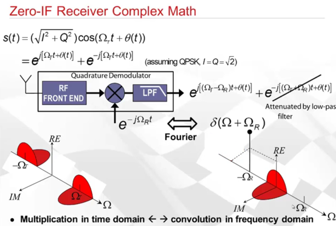
The above figure shows Direct conversion IF to Bits signal chain also known as Zero-IF.
At Receiver:
Incoming RF is converted to baseband using IQ Quadrature demodulator. Dual ADC takes in pair of analog signals I and Q. Taken together I and Q are referred to as complex signal.
According to Nyquist: sampling rate = 2*b/w of signal (centered at DC)
In practice, sampling rate has margin beyond the half signal b/w to accomodate finite role of any anti-aliasing filter.
At Transmitter:
In figure above we have final stage of Direct conversion transmitter with dual DAC and an analog IQ modulator.
This architecture is called direct up conversion because two components I and Q of the complex signal are generated by FPGA and a re converted to analo through DAC's.
Dual DAC is used i.e. 2 DAC's in one IC to reduce phase and gain error b/w analog I and Q components.
IQ modulator forms product of analog signal and a RF carrier of frequency w0. Thereby, shifting the complex spectrum to some RF band suitable for propagation over the air.
RF b/w - 400Mhz to 4GHz
s(t) is the transmitted RF signal represented in complex form as a result of just real part only.
In digital modlation, I and Q form the components of vectors called symbols represented in a 2-D space called constellation. shown in fig is a QPSK, a type of digital modulation whcih encodes 2 bits/symbol resulting in 4 points on the constellation.
In refernece designs, information orginates from hardware based pseudorandom number generators in Zynq Soc or the serial to parallel operations form QPSK symbols.
I and Q takes on values +d or -d base don the bits in the information stream.
Lower bottom equation gives the alernate representation of the output RF signal. We have expressed phase as a function of time in the new expression, to emphasize that the information resides in the instantaneous phase of the carrier, hence the term phase shift keying.
In practice, I and Q signals will be routed through a Digital Up Converter that serves to increase the sampling rate to the DAC while also performing pulse shaping through a digital filter. Shown in figure is a interpolator followed by a single filter, but a Digital up converter consists of cascade of multirate filters.
The received RF signal s(t) is then fed to the IQ Demodulator. The top part is multiplied by the local oscillator at the same RF frequency w0 while the bottom leg is multiplied by the oscillator, that is 90 degrees lagging version. Low pass filtering the output of IQ demodulator leaves the complex message in baseband at 2 separate signal paths I and Q and we are left with I+jQ spectrum sent by transmitter. The analog I and Q generated by IQ Demodulator is then fed to the two ADC's. Due to quadrature demodulator there is always some amount of gain or phase imbalance which can degrade receiver performance but recently due to good quality IQ demodulator direct down conversion is gaining popularity these days.
2 ways to implement quadrature demodulation (analog or digital)
Popular alternative to direct conversion is the I/F sampling
It requires higher ADC analog bandwidth to cover I/F frequency. It uses single ADC that produces the so called real signalthat carries the two I and Q signals in quadrature. DIgital signal processing in the FPGA recovers the I and Q components thereby elimination any error in phase and gain imbalance.
FMCOMMS uses the direct conversion method.
Transmit Path:
Takes complex I and Q signal from system memory and converts into apprporiate RF signal.
AD9122 dual DAC interpolates the data and can apply frequency translation to the baseband data, shifting fundamental signal away from DC.
Complex analog o/p from the DAC feeds quadrature modulator.via an appropriate filter and matching stage where it is translated to a specific RF output frequency.
AD9122 DAC runs at a maximum of 1000MSPS because this is the max clock that can be provided by the AD9523-1.
Receive Path:
IQ demodulator which demodulates the RF signal to suitable complex IF from 50-200MHz.I and Q signals are nexr filtered and then passed to an AD8366 digital variable gain amplifier whcih provides 15.75 dB of gain. An antialias filter is used to remove harmonics and other out of band signals before this signal is digitized by AD9643 and then forwarded to an FPGA or memory.
Control of the registers on the FMCOMMS board is dpne using the I2C from the Zynq Soc.
How FMCOMMS receives data from video 2 next
System can be connected in loop back mode.
Transmit Side:
Sinusoidal tones generated in Direct Digital Synthesizer (DDS). These signals sent to DAC through DAC interface. DAC interface is a custom PCORE created by Analog Devices specially for their high speed DAC's.
Other data path
Processing System --> VDMA(Video Direct Memory Access) --> DAC Interface
VDMA provides high bandwidth direct memory access between external memory and DAC interface.
DAC analog outputs --> IQ modulator (do complex multiplication with an RF carrier, 2.4 GHz)
Receive Side:
Received signal restored to baseband IQ signals using IQ demodulator and then fed to ADC to be digitized through dual ADC. Digital I and Q data streams captured by the ADC interface and sent to external DDR3 memory using DMA.
With access to received I and Q data in DDR3 memory we can plot the data in Matlab.
--------------------------------------------------------------------------------------------------------------------------
Compare what is the I and Q output on the normal QPSK?
Lookout for a simple QPSK
we need some smaller and energy efficient microprocessors to support mobile computing,, electronics quality control
ReplyDelete